One hardware-native ontology.
Every design artifact joins one graph, and three agent modules — Structure, Generate, Verify — run on top of it. Below, what each module takes in and what it puts out.
- 01
Structure
unstructured drawings → AI-readable graph
See how - 02
Generate
specs & drafts, tailored to each use case
See how - 03
Verify
logical errors & omissions — with cited evidence
See how
Three modules · One design graph · On-premises
Messy in. Structured out.
Unstructured design artifacts — documents, datasheets, diagrams, RTL — are parsed into structured design data where every value carries its source page. Diagrams become graphs of nodes and connections; RTL becomes an IP hierarchy.
Input — datasheet, as published
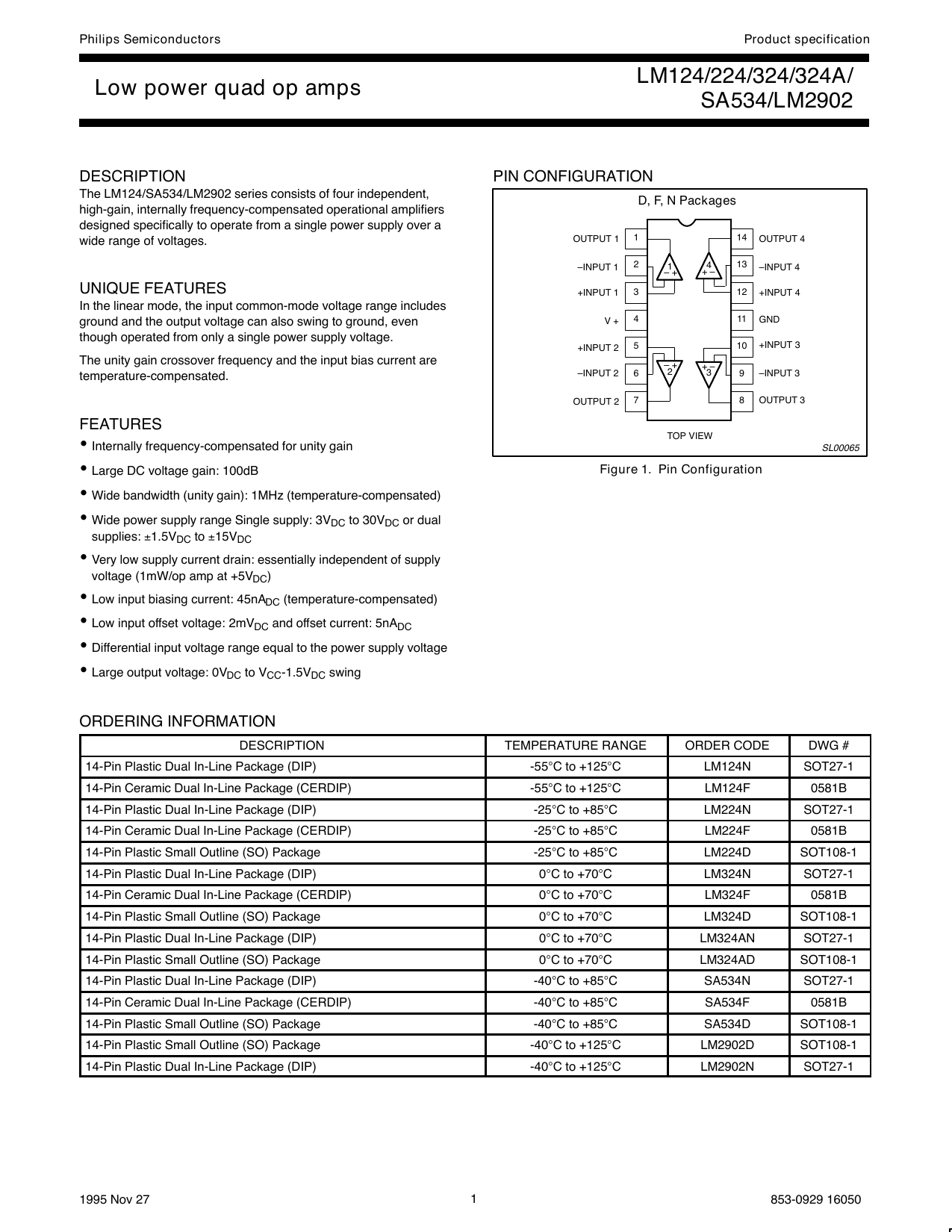
Philips LM124 family — public datasheet
Structured spec
100% source-linked- supply_voltagep.1
3 – 30 V
- gain_dcp.1
100 dB
- pinsp.1
14 — OUT · IN± · V+ · GND
- packagep.1
DIP-14 · SO-14
Functional hierarchy
netlist-ready- TOP — LM124 · quad op amp
- AMP ×4 — identical amplifier blocks
- INPUT — Q1–Q4 differential pair
- GAIN — Q10–Q12 · Cc
- OUTPUT — Q5–Q7 · Q13
- BIAS — 6 µA · 100 µA current sources
Requirements in. Block diagram out.
A reasoning model reads each requirement and updates the architecture tree as it goes, assembles the architecture from circuit blocks proven in past designs, then pins a real, purchasable part to every block against datasheet parameters.
Input — five natural-language requirements
- R112 V battery direct input, reverse-polarity protected
- R24-channel sensor amplification, 12-bit ADC
- R3Operating temperature −40 to +125 °C
- R4CAN FD link, 100 ms status cycle
- R5Standby current ≤ 5 mA
Reasoning log
- › R1 → reverse-polarity P-FET + TVS, buck to 5 V rail
- › R2 → quad op amp + 12-bit ADC on MCU
- › R3 → automotive-grade constraint on every block
- › R4 → CAN FD transceiver + termination
- › R5 → supervisor / watchdog, low-Iq LDO
Output — architecture → parts pinned
parts verifiedCandidates — Quad Op Amp
R3: −40 ~ +125 °C- LM3244ch0 ~ +70 °Crejected — temp range
- LM2244ch−25 ~ +85 °Crejected — temp range
- SA5344ch−40 ~ +85 °Crejected — temp range
- LM29024ch−40 ~ +125 °Cselected · automotive grade
Errors caught before they ship.
Test cases are generated from each requirement; design rules become automatically checkable assertions, verified one by one. Regression runs against the product line's defect history, and failure-mode analysis (FMEDA) surfaces faults the system cannot detect. Every verdict cites its evidence.
DUT — design under test
2 logical design errors · 1 undetectable faultTest cases — generated from R1–R5
- TC-01reverse battery −12 V · 60 s hold · no damagefrom R1
- TC-024-ch ADC sweep · 12-bit code integrityfrom R2
- TC-03temp corners −40 / +25 / +125 °C functionalfrom R3
- TC-04CAN FD status frame period 100 msfrom R4
Assertions — design rules as checks
- assert (nrst has pull-up)pass
- assert (wdt_kick within 100 ms)fail
- assert (can_h / can_l terminated 120 Ω)fail
FMEDA — failure mode, effects & diagnostic analysis
| Element | Failure mode | Effect | Diagnostic | Status |
|---|---|---|---|---|
| Q1 P-FET | short | loss of reverse protection | none | Undetected |
| U1 Buck | output drift | 5V0 overvoltage | U6 supervisor | Detected |
We are building a design-specialized foundation model
that understands requirements through physical layout.
Training data
RTLBehavior · control
always @(*) begin
  if (a) y = b & c;
  else   y = d | e;
end
NetlistFlattened · gates · nets
wire n1, n2;
AND2_X1 g1 (.A1(b), .A2(c), .ZN(n1));
OR2_X1  g2 (.A1(d), .A2(e), .ZN(n2));
MUX2_X1 g3 (.S(a), .A(n2), .B(n1), .Z(y));
LayoutArea · placement · routing
die 2.4 × 1.6 mm
macro A0 @ (120, 80) rot 0
M3 route n1: (12,4)→(48,4)
via M2/M3 @ (48,4)
Circuit Foundation Model
Logical view
Logical representation
Physical view
Physical representation
Requirements → logic → physical, joined in one representation space
Enterprise design workflow · on-premises
- Design generation
- Cross-domain check
- Adapts & learns on in-house data
Logical and physical views of the same circuit meet in one model space — any divergence is caught as a logical design error.
Agents execute.
Engineers lead.
A handful of sample artifacts is enough. We will show you what gets caught in your own data.